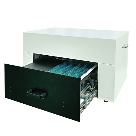
IC Inspection
| Item No.: | 10-3,IC Flaw Inspection System |
Supplier Details
Country: Taiwan
City: Hsinchu City 30075
Address: No. 6, Industry East Road 3, Science Based Industrial Park
TEL: +886-3-5772155
Fax: +886-3-5772598

Online Showroom:
55 Products
IC Flaw Inspection System
Abstract
Non-contact image capturing can be used for inspecting large volumes of chips at one time.
Introduction
IC chips are small in size, delicate in structure, and large in production; therefore, there are needs for accurate and efficient tools to assist in quality inspection. The Inspecting Solution for Defects of IC appearances is by using of a non-contact object scanner, exclusively designed by Microtek, to capture images of IC chips, effectively avoiding misjudgments caused by damaging of IC chips. The object scanner is capable to capture large-scale sizes of images and thus it can handle large volumes of chips fast at one time, shortening inspecting time effectively.
Using together with the MiQC-IC, a defect inspection and management system, a golden sample can be easily selected by an operator. Plus, advanced technology in use, the defective area can be found and marked precisely. After images with defects have been uploaded to the management system, users can find what they are looking for from tones of data quickly by using of file names, uploading dates or defect information, enhancing the management more effective and efficient.
Features
Specifications
Scanning Area: 52 x 38 cm
Working Distance: 7 cm
Scanning Resolution: 20 μm
Image Sensor Type: Color linear CCD
Abstract
Non-contact image capturing can be used for inspecting large volumes of chips at one time.
Introduction
IC chips are small in size, delicate in structure, and large in production; therefore, there are needs for accurate and efficient tools to assist in quality inspection. The Inspecting Solution for Defects of IC appearances is by using of a non-contact object scanner, exclusively designed by Microtek, to capture images of IC chips, effectively avoiding misjudgments caused by damaging of IC chips. The object scanner is capable to capture large-scale sizes of images and thus it can handle large volumes of chips fast at one time, shortening inspecting time effectively.
Using together with the MiQC-IC, a defect inspection and management system, a golden sample can be easily selected by an operator. Plus, advanced technology in use, the defective area can be found and marked precisely. After images with defects have been uploaded to the management system, users can find what they are looking for from tones of data quickly by using of file names, uploading dates or defect information, enhancing the management more effective and efficient.
Features
- Non-contact capturing of images ensures the completeness of scanned objects
- Capturing of a large-scale image enhances the work efficiency for large volumes of chips
- Supports image scanning of various IC chips
- Capable to select a golden sample manually; then, the system will mark positions for all chips and start defect comparisons automatically
- Capable to perform Smart Search by using odd numbers, inspecting items, or point reading
- Capable to set up defect categories and to perform a specific search by using defect items or uploading dates
- Exclusively-designed inspection software can be set up to use on PC and web
Specifications
Scanning Area: 52 x 38 cm
Working Distance: 7 cm
Scanning Resolution: 20 μm
Image Sensor Type: Color linear CCD
 English
 中文繁體
中文繁體 Русско
 Deutsch
 Español
 Português
 Français
 Türk
Türk Italiano
 Nederlands
 हिन्दी
 Bahasa Indonesia
 Tiếng Việt
